


Tesla AI Day and Dojo chip


Lexus Test Driver
Joined: Jan 2007
Posts: 7,460
Likes: 232
From: CA

The SOC uses ARM CPUs, some cheap GPU (not nVidia), and the two NPU cores are custom simplified nvidia rip offs.
No they don't, they don't even have a spec sheet on the single chip lol. The "functioning" tile is just a rendering and a machined metal brick. Would you remind me please, when was the last time anything Tesla announced actually materialized?
No they don't, they don't even have a spec sheet on the single chip lol. The "functioning" tile is just a rendering and a machined metal brick. Would you remind me please, when was the last time anything Tesla announced actually materialized?


Lexus Test Driver


Joined: Feb 2002
Posts: 8,216
Likes: 250
From: New York
Give the dude some credit.
Oh ye his rockets are also used to go to space.
There were many ppl that thought those were pipe dreams too.
So far he has produced everything he promised just not in the timeframe he hoped.
You are focusing on minor nonsense imo - the real value is the AI data Tesla already has and the AI software it developed. This AI day was a showcase to show that Tesla is more than just auto manufacturer, I don’t think anyone is thinking we are going to get a Tesla bot next year to do our grocery shopping. 😀
Do you realize that Musk launched a full scale Auto manufacturing company from scratch?!
Give the dude some credit.
Oh ye his rockets are also used to go to space.
There were many ppl that thought those were pipe dreams too.
So far he has produced everything he promised just not in the timeframe he hoped.
You are focusing on minor nonsense imo - the real value is the AI data Tesla already has and the AI software it developed. This AI day was a showcase to show that Tesla is more than just auto manufacturer, I don’t think anyone is thinking we are going to get a Tesla bot next year to do our grocery shopping. 😀
Give the dude some credit.
Oh ye his rockets are also used to go to space.
There were many ppl that thought those were pipe dreams too.
So far he has produced everything he promised just not in the timeframe he hoped.
You are focusing on minor nonsense imo - the real value is the AI data Tesla already has and the AI software it developed. This AI day was a showcase to show that Tesla is more than just auto manufacturer, I don’t think anyone is thinking we are going to get a Tesla bot next year to do our grocery shopping. 😀
Full credit where its due, but there are very many of his promises that never materialized, and I'm not talking about the silly robot. It's best not to hold your breath for anything they announce.


You don’t even see this inside any mobile phones. Imagine Apple makes all pcb and chip packages disappeared and how much more space you can have for bigger battery and more sensors for the phone?
Abstract:
A novel wafer-scale system integration solution, InFO_SoW (System-on-Wafer), has been successfully developed to integrate known-good chips arrays with power and thermal module for high performance computing. InFO_SoW eliminates the use of substrate and PCB by serving as the carrier itself. Close packed multiple chips arrays within a compact system enable the solution to reap the wafer-scale benefits such as low latency chip-to-chip communication, high bandwidth density and low PDN impedance for greater computing performance and power efficiency. In addition to heterogeneous chips integration, its wafer-field processing capability has enabled chiplet-based design for greater cost saving and design flexibility.This paper demonstrated the industry's first wafer-scale system integration package with InFO technology. Electrical characterization results revealed good process uniformity across the super large package of InFO_SoW. It is simulated to have about 15 % power saving of the interconnects with length of 30 mm due to lower surface roughness of InFO RDL. Thermal management of such high power in a compact system has been validated through scalable proof-of-concept (POC) thermal solution. The POC thermal solution proved its capability of dissipating 7000 W out of the 2-by-5 array dummy heater, whereby the maximal temperature of the dummy heater is kept below 90°C. In addition, InFO_SoW structural robustness has been verified through both InFO wafer-level quick torture and system-level reliability tests. Despite its super large package size, thermomechanical Chip-Package-Interaction (CPI) simulation study revealed that InFO_SoW has relatively low risk when compared to qualified Flip-Chip package with advanced Si-node.
Published in: 2020 IEEE 70th Electronic Components and Technology Conference (ECTC)
I found the answer. They’re bypassing chip packages and PCB all together and put array of die on a fan out wafer. I haven’t seen something like this. Unless Tesla has really figured this out or like you said smokes and mirrors concept that might never happen. Something like this isn’t easy to do, interconnect industries have been trying to do this for yrs. Below is possible tech they’re using…
You don’t even see this inside any mobile phones. Imagine Apple makes all pcb and chip packages disappeared and how much more space you can have for bigger battery and more sensors for the phone?
Abstract:
A novel wafer-scale system integration solution, InFO_SoW (System-on-Wafer), has been successfully developed to integrate known-good chips arrays with power and thermal module for high performance computing. InFO_SoW eliminates the use of substrate and PCB by serving as the carrier itself. Close packed multiple chips arrays within a compact system enable the solution to reap the wafer-scale benefits such as low latency chip-to-chip communication, high bandwidth density and low PDN impedance for greater computing performance and power efficiency. In addition to heterogeneous chips integration, its wafer-field processing capability has enabled chiplet-based design for greater cost saving and design flexibility.This paper demonstrated the industry's first wafer-scale system integration package with InFO technology. Electrical characterization results revealed good process uniformity across the super large package of InFO_SoW. It is simulated to have about 15 % power saving of the interconnects with length of 30 mm due to lower surface roughness of InFO RDL. Thermal management of such high power in a compact system has been validated through scalable proof-of-concept (POC) thermal solution. The POC thermal solution proved its capability of dissipating 7000 W out of the 2-by-5 array dummy heater, whereby the maximal temperature of the dummy heater is kept below 90°C. In addition, InFO_SoW structural robustness has been verified through both InFO wafer-level quick torture and system-level reliability tests. Despite its super large package size, thermomechanical Chip-Package-Interaction (CPI) simulation study revealed that InFO_SoW has relatively low risk when compared to qualified Flip-Chip package with advanced Si-node.
Published in: 2020 IEEE 70th Electronic Components and Technology Conference (ECTC)
You don’t even see this inside any mobile phones. Imagine Apple makes all pcb and chip packages disappeared and how much more space you can have for bigger battery and more sensors for the phone?
Abstract:
A novel wafer-scale system integration solution, InFO_SoW (System-on-Wafer), has been successfully developed to integrate known-good chips arrays with power and thermal module for high performance computing. InFO_SoW eliminates the use of substrate and PCB by serving as the carrier itself. Close packed multiple chips arrays within a compact system enable the solution to reap the wafer-scale benefits such as low latency chip-to-chip communication, high bandwidth density and low PDN impedance for greater computing performance and power efficiency. In addition to heterogeneous chips integration, its wafer-field processing capability has enabled chiplet-based design for greater cost saving and design flexibility.This paper demonstrated the industry's first wafer-scale system integration package with InFO technology. Electrical characterization results revealed good process uniformity across the super large package of InFO_SoW. It is simulated to have about 15 % power saving of the interconnects with length of 30 mm due to lower surface roughness of InFO RDL. Thermal management of such high power in a compact system has been validated through scalable proof-of-concept (POC) thermal solution. The POC thermal solution proved its capability of dissipating 7000 W out of the 2-by-5 array dummy heater, whereby the maximal temperature of the dummy heater is kept below 90°C. In addition, InFO_SoW structural robustness has been verified through both InFO wafer-level quick torture and system-level reliability tests. Despite its super large package size, thermomechanical Chip-Package-Interaction (CPI) simulation study revealed that InFO_SoW has relatively low risk when compared to qualified Flip-Chip package with advanced Si-node.
Published in: 2020 IEEE 70th Electronic Components and Technology Conference (ECTC)
Lexus Test Driver
Joined: Jan 2007
Posts: 7,460
Likes: 232
From: CA
I found the answer. They’re bypassing chip packages and PCB all together and put array of die on a fan out wafer. I haven’t seen something like this. Unless Tesla has really figured this out or like you said smokes and mirrors concept that might never happen. Something like this isn’t easy to do, interconnect industries have been trying to do this for yrs. Below is possible tech they’re using…
You don’t even see this inside any mobile phones. Imagine Apple makes all pcb and chip packages disappeared and how much more space you can have for bigger battery and more sensors for the phone?
Abstract:
A novel wafer-scale system integration solution, InFO_SoW (System-on-Wafer), has been successfully developed to integrate known-good chips arrays with power and thermal module for high performance computing. InFO_SoW eliminates the use of substrate and PCB by serving as the carrier itself. Close packed multiple chips arrays within a compact system enable the solution to reap the wafer-scale benefits such as low latency chip-to-chip communication, high bandwidth density and low PDN impedance for greater computing performance and power efficiency. In addition to heterogeneous chips integration, its wafer-field processing capability has enabled chiplet-based design for greater cost saving and design flexibility.This paper demonstrated the industry's first wafer-scale system integration package with InFO technology. Electrical characterization results revealed good process uniformity across the super large package of InFO_SoW. It is simulated to have about 15 % power saving of the interconnects with length of 30 mm due to lower surface roughness of InFO RDL. Thermal management of such high power in a compact system has been validated through scalable proof-of-concept (POC) thermal solution. The POC thermal solution proved its capability of dissipating 7000 W out of the 2-by-5 array dummy heater, whereby the maximal temperature of the dummy heater is kept below 90°C. In addition, InFO_SoW structural robustness has been verified through both InFO wafer-level quick torture and system-level reliability tests. Despite its super large package size, thermomechanical Chip-Package-Interaction (CPI) simulation study revealed that InFO_SoW has relatively low risk when compared to qualified Flip-Chip package with advanced Si-node.
Published in: 2020 IEEE 70th Electronic Components and Technology Conference (ECTC)
You don’t even see this inside any mobile phones. Imagine Apple makes all pcb and chip packages disappeared and how much more space you can have for bigger battery and more sensors for the phone?
Abstract:
A novel wafer-scale system integration solution, InFO_SoW (System-on-Wafer), has been successfully developed to integrate known-good chips arrays with power and thermal module for high performance computing. InFO_SoW eliminates the use of substrate and PCB by serving as the carrier itself. Close packed multiple chips arrays within a compact system enable the solution to reap the wafer-scale benefits such as low latency chip-to-chip communication, high bandwidth density and low PDN impedance for greater computing performance and power efficiency. In addition to heterogeneous chips integration, its wafer-field processing capability has enabled chiplet-based design for greater cost saving and design flexibility.This paper demonstrated the industry's first wafer-scale system integration package with InFO technology. Electrical characterization results revealed good process uniformity across the super large package of InFO_SoW. It is simulated to have about 15 % power saving of the interconnects with length of 30 mm due to lower surface roughness of InFO RDL. Thermal management of such high power in a compact system has been validated through scalable proof-of-concept (POC) thermal solution. The POC thermal solution proved its capability of dissipating 7000 W out of the 2-by-5 array dummy heater, whereby the maximal temperature of the dummy heater is kept below 90°C. In addition, InFO_SoW structural robustness has been verified through both InFO wafer-level quick torture and system-level reliability tests. Despite its super large package size, thermomechanical Chip-Package-Interaction (CPI) simulation study revealed that InFO_SoW has relatively low risk when compared to qualified Flip-Chip package with advanced Si-node.
Published in: 2020 IEEE 70th Electronic Components and Technology Conference (ECTC)

https://www.datacenterdynamics.com/e...g-tile-module/
They already have a working training tile with silicon. Och thinks they are lying but they showed off the tile at the event. Its Teslas word against his I guess
https://www.datacenterdynamics.com/e...g-tile-module/
https://www.datacenterdynamics.com/e...g-tile-module/
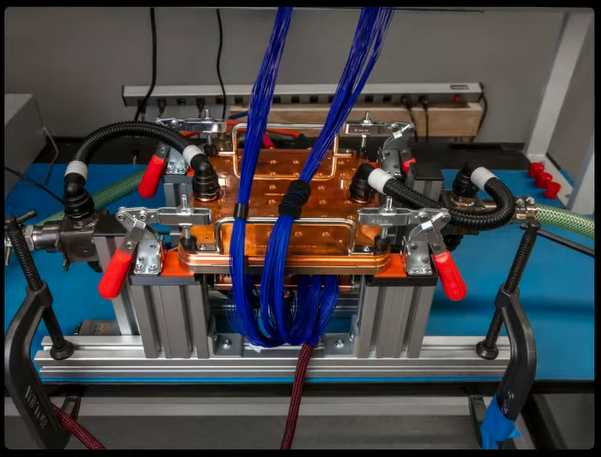
Yeah, a low res photo of a brass plate clamped down to scrap aluminum profiles with c-clamps, a garden hose, and some cables capable of maybe 1kw. And a power strip on top of a 2x4 in the back ground. Looks totally legit, how do I preorder?
Lexus Test Driver
Joined: Jan 2007
Posts: 7,460
Likes: 232
From: CA
But keep it going...highly entertaining.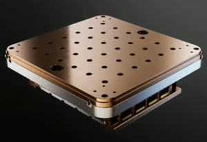
Lol. The actual system isn't built so this is a prototype testing unit in a lab environment. Looks a lot like the picture they showed in the presentation. You're just trolling at this point as every publication acknowledges the existence of this hardware But keep it going...highly entertaining.
But keep it going...highly entertaining.This "lab" is just a random table they had in the metal shop where they just machined the copper plate, and then they set up the whole contraption for the photo, while laughing their asses off realizing that 95+ percent of people will think its legit.

They already have a working training tile with silicon. Och thinks they are lying but they showed off the tile at the event. Its Teslas word against his I guess
https://www.datacenterdynamics.com/e...g-tile-module/
https://www.datacenterdynamics.com/e...g-tile-module/
Yes, they designed this in-house which is really impressive but somebody will actually have to make it. I don’t think Tesla can manufacture it. InfoSoW is still a concept from TSMC. New M1 processor from Apple does something like this with RAM die next to their processor die but not at this level. Dojo even has power regulators mounted directly to die. You know it took chip industry a few yrs just to put capacitors directly inside chip packages.
https://semianalysis.com/tesla-ai-da...tsmc-info_sow/
The article said what we already know but I’m honestly curious of the hardware whether they really have working one. Lab hardware are always huge and bulky but if they plan to put one inside Tesla robot it should be really compact like the images they show. Maybe we are still yrs off 10-15 yrs but the purpose of just training AI with Dojo they can get away with bulky system.
Yes, they designed this in-house which is really impressive but somebody will actually have to make it. I don’t think Tesla can manufacture it. InfoSoW is still a concept from TSMC. New M1 processor from Apple does something like this with RAM die next to their processor die but not at this level. Dojo even has power regulators mounted directly to die. You know it took chip industry a few yrs just to put capacitors directly inside chip packages.
https://semianalysis.com/tesla-ai-da...tsmc-info_sow/
Yes, they designed this in-house which is really impressive but somebody will actually have to make it. I don’t think Tesla can manufacture it. InfoSoW is still a concept from TSMC. New M1 processor from Apple does something like this with RAM die next to their processor die but not at this level. Dojo even has power regulators mounted directly to die. You know it took chip industry a few yrs just to put capacitors directly inside chip packages.
https://semianalysis.com/tesla-ai-da...tsmc-info_sow/